Flexibility of our Plating Service
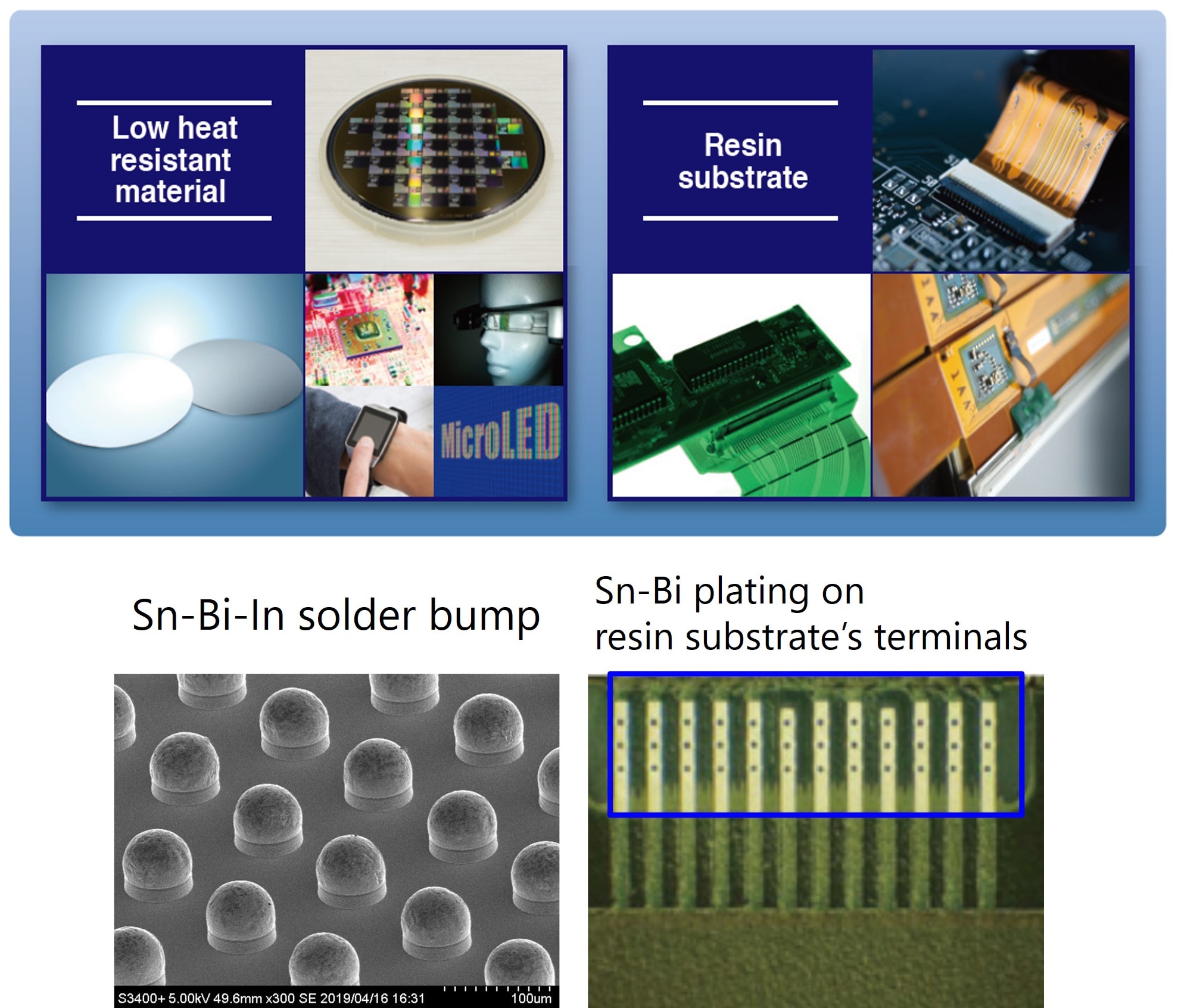
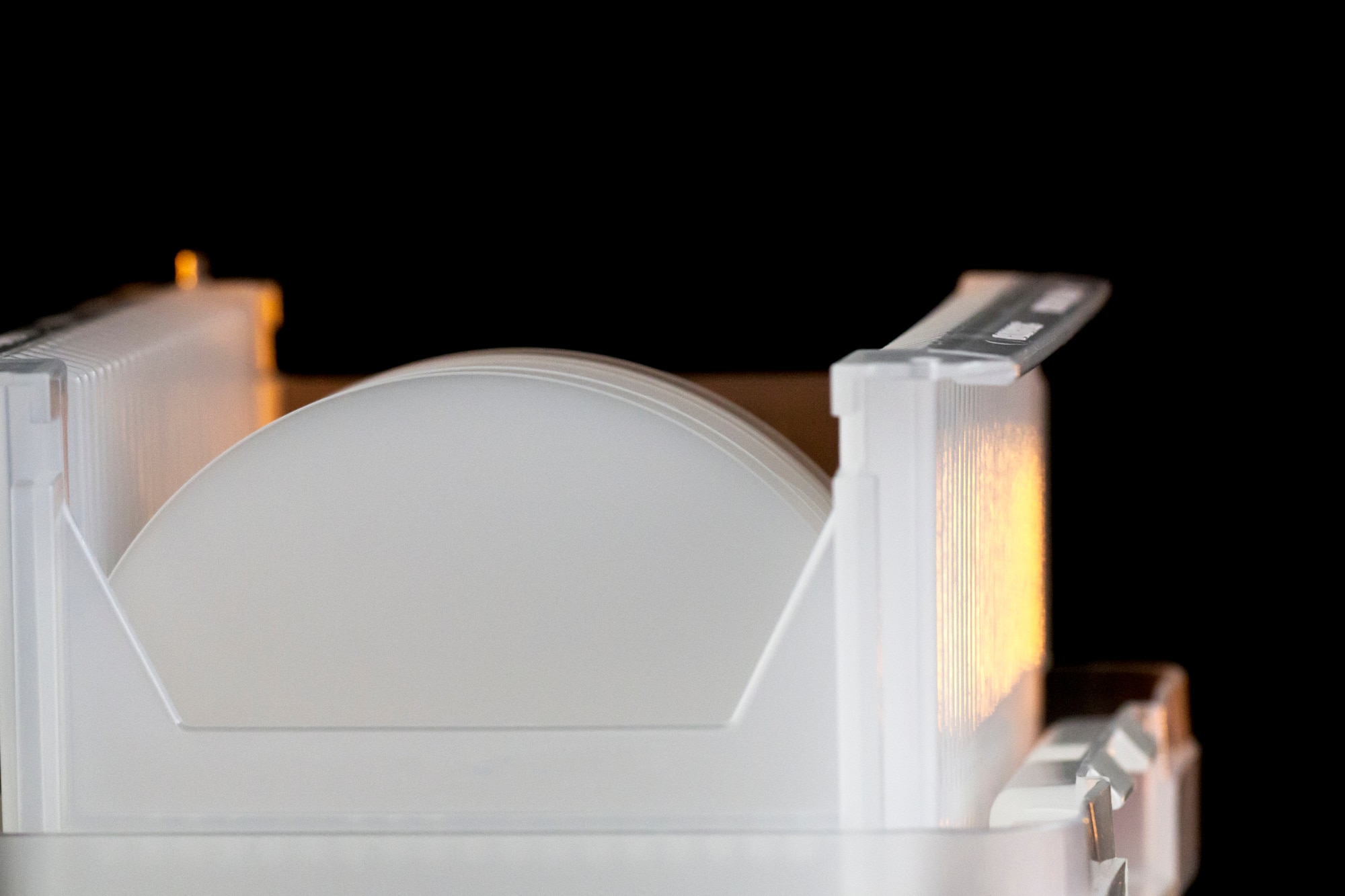
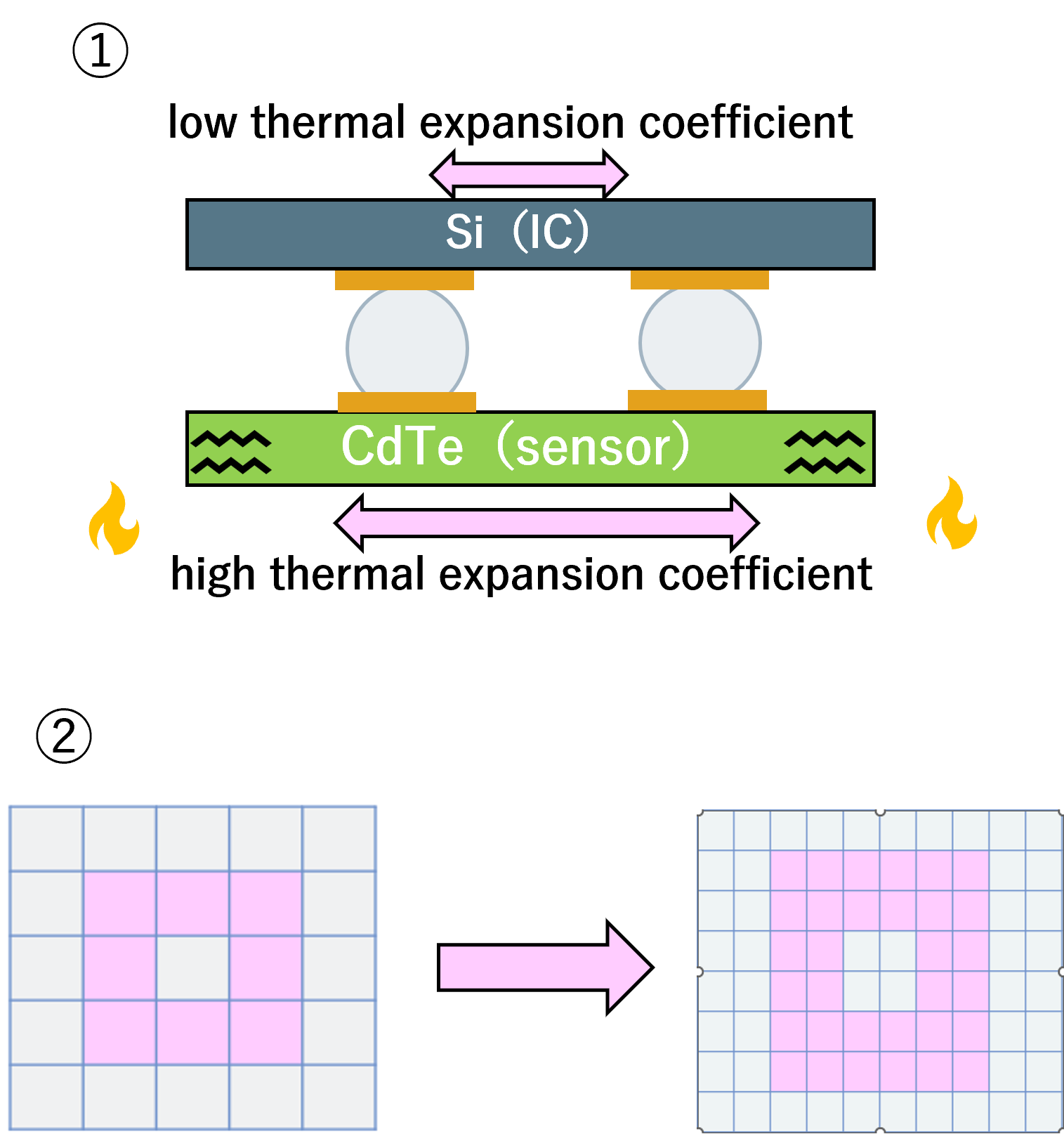
We accept not only Si wafers, but also other types of wafers such as glass, SiC for power devices, InP and GaAs for photonics and communication devices, and panel substrates for chiplet and heterogeneous integration packaging.
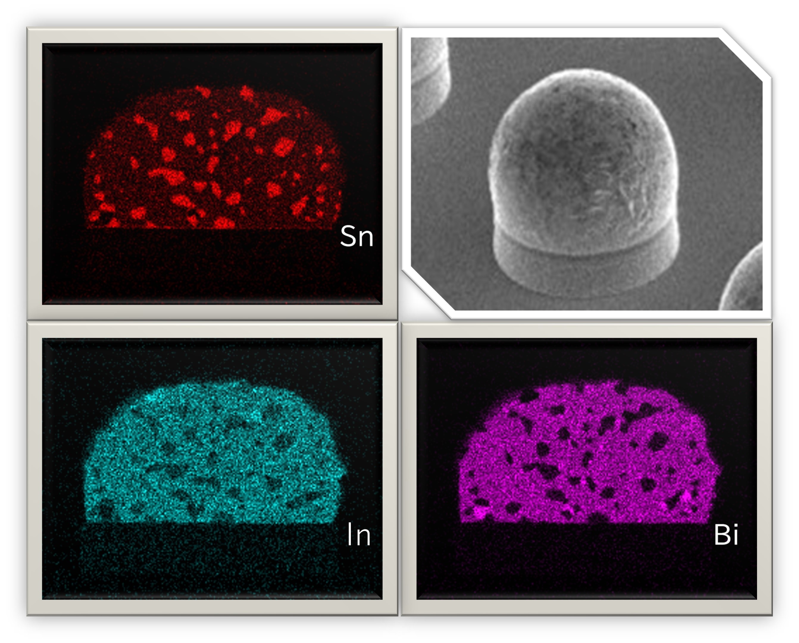
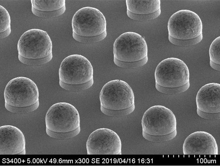
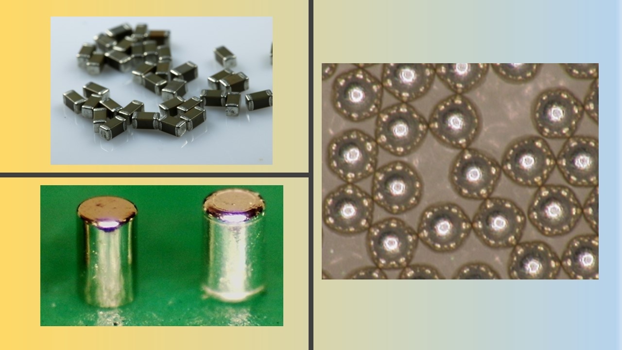
Other than wafers and substrates, we also undertake plating on small components like Cu core balls, metal powders, and wires.
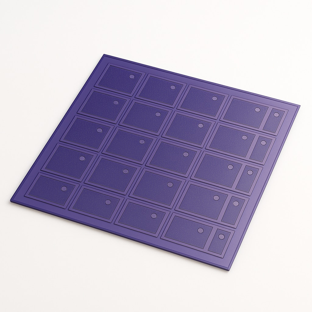
Shinryo is happy to help our customers from the trial stage, so we gladly accept even 1 wafer or 1 lot of the components for a trial. When you do not have wafers for TEG production, we can prepare them ourselves. Please feel free to ask.